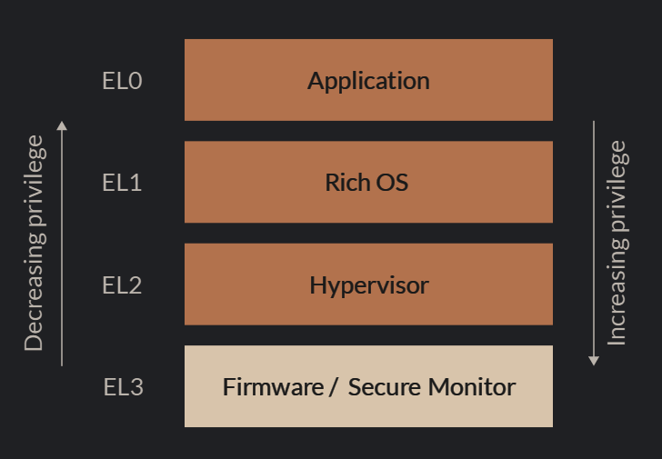
 1 – Exception levels
Movement between ELs occurs when taking, or returning from, an
exception. The general rule is that on taking an exception, the EL can
only stay the same or go up; on returning from an exception, it can only
stay the same or go down.[^4]
Note that the architecture defines these four ELs but does not mandate
the use of each level. The model in Figure 1 is, however, common and
typical. Also, while support of EL0 and EL1 is mandatory in any
implementation, EL2 and EL3 are optional. In practice, these levels are
usually implemented, since EL2 supports the virtualization features
required by most hypervisors, and EL3 is the only EL which can change
security state.
### 4.1.2 Execution States and Instruction Sets
Armv8–A and Armv9–A processors support two execution states: AArch32, a
32-bit execution state; and AArch64, a 64-bit execution state. In
general, the execution state defines the width of the general–purpose
register set, and also the available instruction sets.
In Armv8–A, either or both execution states may be supported at each
exception level. Armv9 –A requires that AArch64 is supported at all ELs,
while AArch32 may be optionally supported only at EL0.
Execution state can only change when the exception level changes, and,
in a similar fashion to exception levels, the architecture requires that
when moving to a higher EL, the execution state may either stay the same
or change to AArch64. On moving to a lower EL, it can either stay the
same or change to AArch64. The rules on changing exception level and
execution state have a number of implications:
- If AArch32 is not implemented at a particular EL, then it cannot be
implemented at any higher levels.
- AArch32 software at any particular EL can only host AArch32 software at
any lower levels.
- An AArch64 operating system executing at EL1 can host both AArch32 and
AArch64 software executing at EL0.
- An AArch64 hypervisor executing at EL2 can host both AArch32 and AArch64
software executing at EL1.
1 – Exception levels
Movement between ELs occurs when taking, or returning from, an
exception. The general rule is that on taking an exception, the EL can
only stay the same or go up; on returning from an exception, it can only
stay the same or go down.[^4]
Note that the architecture defines these four ELs but does not mandate
the use of each level. The model in Figure 1 is, however, common and
typical. Also, while support of EL0 and EL1 is mandatory in any
implementation, EL2 and EL3 are optional. In practice, these levels are
usually implemented, since EL2 supports the virtualization features
required by most hypervisors, and EL3 is the only EL which can change
security state.
### 4.1.2 Execution States and Instruction Sets
Armv8–A and Armv9–A processors support two execution states: AArch32, a
32-bit execution state; and AArch64, a 64-bit execution state. In
general, the execution state defines the width of the general–purpose
register set, and also the available instruction sets.
In Armv8–A, either or both execution states may be supported at each
exception level. Armv9 –A requires that AArch64 is supported at all ELs,
while AArch32 may be optionally supported only at EL0.
Execution state can only change when the exception level changes, and,
in a similar fashion to exception levels, the architecture requires that
when moving to a higher EL, the execution state may either stay the same
or change to AArch64. On moving to a lower EL, it can either stay the
same or change to AArch64. The rules on changing exception level and
execution state have a number of implications:
- If AArch32 is not implemented at a particular EL, then it cannot be
implemented at any higher levels.
- AArch32 software at any particular EL can only host AArch32 software at
any lower levels.
- An AArch64 operating system executing at EL1 can host both AArch32 and
AArch64 software executing at EL0.
- An AArch64 hypervisor executing at EL2 can host both AArch32 and AArch64
software executing at EL1.
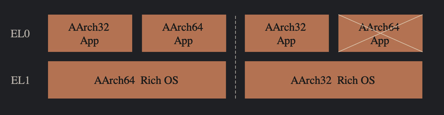 Figure 2– Exception levels and Execution States
In AArch32:
- Operation is backwards-compatible with Armv7–A and previous
architectures.
- The A32 and T32 instruction sets are available.[^5]
- The 32–bit Armv7–A register set is supported.
In AArch64:
- Only the A64 instruction set is available.
- The general-purpose register set is expanded, both in width and in
number, compared to Armv7–A and earlier architectures.
A32 is the direct descendant of the original instruction set used by the
earliest Arm processors. In A32, all instructions are 32 bits wide and
are aligned on 32-bit address boundaries in memory.
T32 evolved from the Thumb instruction set introduced in the
Arm7TDMI® (architecture Armv4T). For more detail on the
origins of the Thumb instruction set, see §3.2 above. In the original
Thumb instruction set, all instructions are 16 bits wide and are aligned
on even address boundaries. These instructions form a 16-bit encoded
subset of the Arm instruction set, and each instruction has a direct Arm
equivalent.[^6]
The original Thumb instruction set was significantly expanded, initially
in the Arm1156–T2 processor, by addition of some 32-bit instructions,
yielding a mixed-length instruction set originally known as Thumb–2.
This instruction set has evolved into what is now called T32.
A64 is an entirely new instruction set introduced in Armv8–A, and
carried forward into Armv9–A.
Within AArch32 state, the A32 and T32 instruction sets each have an
associated “state”—Arm state for A32, and Thumb state for T32. These are
indicated by the value of the T bit within the CPSR. A change of state
can only be caused by a branch or return instruction, or on entry to, or
return from, an exception.
### 4.1.3 Security States
Most Cortex–A processors support two security states: Secure and
Non-Secure.[^7] Certain processor features are architecturally
classified as Secure and can only be accessed by software executing in
Secure state. Secure state information is also propagated outside the
processor into external components such as the memory interface, caches,
memory management units, and other peripherals. This allows system
designers to partition the system into sets of Secure and Non-Secure
components.
When executing in Secure state, software can access both Secure and
Non-Secure components and features; when executing in Non-Secure state,
Secure items cannot be accessed and attempts to do so will usually
result in an exception.
This architecture allows the implementation of secure subsystems within
the system. This might be, for example, a secure payment or DRM
subsystem executing in Secure state and using some secure features,
alongside an operating system such as Linux or Android, executing in
Non-Secure state. As long as the mechanism for changing security state
is strongly protected, this prevents Non-Secure software from accessing
or observing Secure software and hardware. In an Armv8–A or Armv9–A
system, the only route into Secure state is through a Secure Monitor,
which executes in EL3. An example system configuration is shown in
Figure 3.
Figure 2– Exception levels and Execution States
In AArch32:
- Operation is backwards-compatible with Armv7–A and previous
architectures.
- The A32 and T32 instruction sets are available.[^5]
- The 32–bit Armv7–A register set is supported.
In AArch64:
- Only the A64 instruction set is available.
- The general-purpose register set is expanded, both in width and in
number, compared to Armv7–A and earlier architectures.
A32 is the direct descendant of the original instruction set used by the
earliest Arm processors. In A32, all instructions are 32 bits wide and
are aligned on 32-bit address boundaries in memory.
T32 evolved from the Thumb instruction set introduced in the
Arm7TDMI® (architecture Armv4T). For more detail on the
origins of the Thumb instruction set, see §3.2 above. In the original
Thumb instruction set, all instructions are 16 bits wide and are aligned
on even address boundaries. These instructions form a 16-bit encoded
subset of the Arm instruction set, and each instruction has a direct Arm
equivalent.[^6]
The original Thumb instruction set was significantly expanded, initially
in the Arm1156–T2 processor, by addition of some 32-bit instructions,
yielding a mixed-length instruction set originally known as Thumb–2.
This instruction set has evolved into what is now called T32.
A64 is an entirely new instruction set introduced in Armv8–A, and
carried forward into Armv9–A.
Within AArch32 state, the A32 and T32 instruction sets each have an
associated “state”—Arm state for A32, and Thumb state for T32. These are
indicated by the value of the T bit within the CPSR. A change of state
can only be caused by a branch or return instruction, or on entry to, or
return from, an exception.
### 4.1.3 Security States
Most Cortex–A processors support two security states: Secure and
Non-Secure.[^7] Certain processor features are architecturally
classified as Secure and can only be accessed by software executing in
Secure state. Secure state information is also propagated outside the
processor into external components such as the memory interface, caches,
memory management units, and other peripherals. This allows system
designers to partition the system into sets of Secure and Non-Secure
components.
When executing in Secure state, software can access both Secure and
Non-Secure components and features; when executing in Non-Secure state,
Secure items cannot be accessed and attempts to do so will usually
result in an exception.
This architecture allows the implementation of secure subsystems within
the system. This might be, for example, a secure payment or DRM
subsystem executing in Secure state and using some secure features,
alongside an operating system such as Linux or Android, executing in
Non-Secure state. As long as the mechanism for changing security state
is strongly protected, this prevents Non-Secure software from accessing
or observing Secure software and hardware. In an Armv8–A or Armv9–A
system, the only route into Secure state is through a Secure Monitor,
which executes in EL3. An example system configuration is shown in
Figure 3.
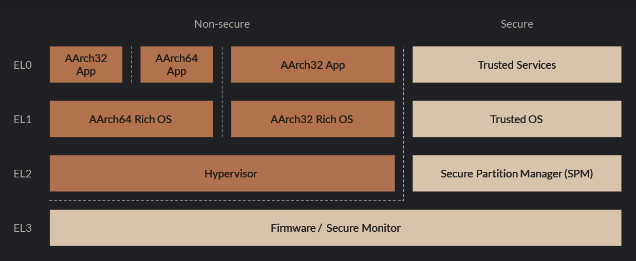 Figure 3 – Exception Levels, Security States and Execution States
Armv9–A extends the security model with the Realm Management Extension
(RME). RME adds two new Security states: Root and Realm. In Root state,
which is only available in EL3, the processor can access the entire
physical address space. In Realm state, the processor can only access
Non-Secure and “Realm” addresses. Real memory accesses are policed by a
separate piece of software called the Realm Manager. Together with
specific RME hardware features, this provides robust
compartmentalization and greatly enhances security. Figure 4 shows an
example configuration when RME is implemented.
Figure 3 – Exception Levels, Security States and Execution States
Armv9–A extends the security model with the Realm Management Extension
(RME). RME adds two new Security states: Root and Realm. In Root state,
which is only available in EL3, the processor can access the entire
physical address space. In Realm state, the processor can only access
Non-Secure and “Realm” addresses. Real memory accesses are policed by a
separate piece of software called the Realm Manager. Together with
specific RME hardware features, this provides robust
compartmentalization and greatly enhances security. Figure 4 shows an
example configuration when RME is implemented.
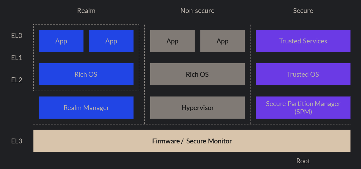 Figure 4 – RME Security States
## 4.2 Armv9.0–A
The Armv9.0–A architecture was announced in 2021, baselined on
Armv8.5–A.
The main drivers for the Armv9 architecture are increased security and
improved vector processing. The major architecture features involved
are:
- Confidential Computer Architecture (CCA)
- Transactional Memory Extension (TME)
- Scalable Vector Extensions V2 (SVE2)
CCA is a major innovation in device security, driven by the
fast-evolving needs of the industry. It was developed in collaboration
with university research partners. CCA provides a compartmentalized
architecture in which processes can execute in “realms”, which are
isolated from each other. As well as hardware support, a standard
firmware architecture is also specified. CCA is a combination of a
number of architecture extensions, including Realm Management Extension
(RME), Dynamic TrustZone® Technology, Real Management Monitor
(RMM), and standard CCA firmware.
TME provides for Hardware Transactional Memory (HTM), which allows
sequences of instructions to be executed by the processor atomically.
This greatly simplifies and enhances the execution of multi–threaded
software on systems that consist of many independent processing
elements. TME builds upon a number of architecture extensions, including
Hardware Transactional Memory (HTM) and Transactional Lock Elision
(TLE).
There are also a number of optional extensions, some of which are
entirely new to the Arm architecture, while others build upon features
from prior architecture versions. These include:
- Armv9 Cryptographic Extensions
- Embedded Trace Extension (ETE)
- Trace Buffer Extension (TBE)
- Scalable Vector Extension V2 (SVE2)
The optional SVE2 extension is an evolution of The SVE vector processing
architecture introduced in Armv8. Extensions to the earlier iteration of
SVE allow for better fine-grained Data Level Parallelism (DLP) making it
easier for compilers to vectorize key algorithms. Support is also
introduced to accelerate key algorithms employed by the widely used
Advanced Encryption Standard (AES).
## 4.3 Armv9.1–A
Armv9.1–A was announced in September 2019 and builds on both Armv9–0–A
and Armv8.6–A. All mandatory features from those two earlier
architectures are also mandatory in Armv9.1–A.
New features introduced include:
- additional floating-point matrix multiply instructions (GEMM);
- extensions to the Embedded Trace Extension introduced in Armv9.0–A; and
- Memory Partitioning and Monitoring (MPAM), which allows the system to
monitor and restrict the memory bandwidth used by individual processes,
in order to manage and mitigate the effect on performance of other
processes.
## 4.4 Armv9.2–A
Armv9.2–A, baselined on Armv8.7–A, was announced in September 2020, and
includes some minor instruction set enhancements, and an extension to
Realm Management. Main changes include:
- Root & Realm security states and physical address spaces;
- Granule Protection Check mechanism;
- enhanced PCIe hot plug;
- atomic 64–byte load/store to accelerators;
- further extensions to ETE to support Realm Management (RME);
- Scalable Matrix Extension (SME) (Optional—allows tiled storage of
vectors in registers);
- Realm Management Extension (RME) (Optional); and
- Branch–Record recording (Optional—captures execution path history).
## 4.5 Armv9.3–A
Armv9.3–A, baselined on Armv8.8–A, was announced in September 2021.
Additions include:
- Branch Recording in EL3;
- “Non–maskable” (NMI) and “less-maskable” interrupts (LMI) for NMI for
AArch64;
- memcpy and memset instructions;
- hinted conditional branches (the ability to include hints with branch
instructions, which helps the branch prediction logic by indicating that
a particular branch is consistent and is unlikely to change direction);
- Scalable Matrix Extensions v2 (Optional), which introduces the ability
to re-address two-dimensional tiles as groups of one–dimensional
vectors; and
- Memory Encryption Contexts (MEC) (Optional)—an extension to RME that
provides additional contexts for memory encryption linked to existing
realms.
## 4.6 Armv9.4–A
Armv9.4–A, baselined on Armv8.9–A, was announced in September 2022.
Additions include:
- improved security against attacks that use branch history to infer and
manipulate execution;
- VMSA enhancements including 128–bit translation tables, system
registers, and atomic 128–bit instructions (Optional);
- SME2 and SVE2.1 (Optional), which add a number of extra instructions to
SME and SVE2 to improve matrix and vector operations; and
- Guarded Control Stack (Optional)—a separate memory area for the storage
of exception returns and branch returns, protected from modification.
## 4.7 Armv9.5–A
Armv9.5–A (October 2023) introduces:
- 8–bit Floating Point (FP8) support added to SME2, SVE2 and Neon™.
## 4.8 Armv9.6–A
Armv9.6–A (October 2024) introduces:
- MPAM Domains for improved support of shared memory in multi-chiplet and
chip systems; and
- Granular Data Isolation for Confidential Compute.
# 5. The Neoverse Cores
So far, you have read about the development of two distinct threads in
the Arm® product range. Firstly, the evolution of the
architecture—the contract between hardware and software that defines the
behavior of devices compatible with Arm architecture. Secondly, the
implementation of a growing range of processor cores based on each
variant of the architecture. These two factors, independent yet related,
are important when understanding the rationale behind each Arm device.
The architecture of a particular device does not dictate what it will be
used for. For example, not all Cortex–A devices are used in mobile
phones, although a great number are. Similarly, not all Armv9–A
processors are used in infrastructure applications, though many of them
are very suitable for this. It is the combination of architecture and
implementation that determines whether it is suitable for a particular
use case.
The Neoverse devices conform to a mixture of architectures. Early cores
were built to Armv8–A, and later cores to Armv9–A, but every
implementation choice was made deliberately to make them suitable for
use in infrastructure applications.
Each Neoverse™ device is different. These differences arise partly from
the architecture, but also from choices made by whoever implements the
device, and the particular manufacturing process used in their
production. Understanding this is important when evaluating or selecting
a device.
It is also important to understand this when reading, in the next
chapter, the list of currently available Neoverse devices. They are
wonderfully diverse, and this diversity is one of the strengths of the
Arm product family.
## 5.1 Architecture, Implementation and Manufacturing
Much of the base functionality of a particular device is defined in the
architecture. While some of it may be optional, it is essentially
immutable. Other behavior is determined by whoever implements or
manufactures the device, and they have significant freedom here.
Some sources make the distinction between architectural,
microarchitectural, and implementational behavior.
### 5.1.1 Architecturally-Defined Behavior
In the preceding sections, you have looked at some of the behaviors that
are mandated by the architecture itself. The consistency across the
product range, enforced by the requirements of the architecture, has
been a key factor in the success of the Arm architecture in the
marketplace. In essence, as you have already seen, the architecture
defines the behavior of the hardware when the hardware is presented with
an instruction or a stream of instructions. The consistent behavior of
all Arm devices conforming to a particular architecture version is
crucial. It ensures consistent software behavior across all
implementations, which is key in establishing a wide and vibrant
ecosystem.
Although the architecture defines the required behavior precisely, it
permits a degree of freedom in many aspects of the final device. For
instance, the architecture defines whether caches are permissible, what
their structure may be, and how they respond to management operations,
but the architecture doesn’t specify their size. That decision, along
with many others, is left to whoever implements the device.
In addition, many architectural features are specified as “optional”.
These relate to features that may or may not be implemented in the
production device, at the discretion of the implementer. However, if
these features are included, the architecture defines precisely how they
must behave. On the other hand, if an “optional” feature is not
implemented, the architecture defines the corresponding behavior in
their absence.
The architecture also defines mechanisms by which software developers
can interrogate the system to determine which optional features are
implemented and with which implementation parameters.
There are several architecture licensees operating in this market space,
and the behavior of their products depends on both the architecture and
on the specific implementation deployed by the licensee. In many cases,
that implementation might be proprietary.
### 5.1.2 Implementation Decisions—Microarchitecture
The process of “implementation” involves taking the HDL source code for
the hardware from Arm and transforming that into a description of a
processing element that can be fabricated into a working, physical
device. This is a highly complex multi-stage process. Significant
choices are made along the way that affect the behavior and capability
of the production device.
Those choices might include:
- whether certain optional architectural features are implemented;
- the size and scope of processor and associated logic, such as caches,
buses, and interconnect architecture;
- the number and organization of processing elements; and
- the length and structure of the processor pipeline.
Clearly, these features have a considerable effect on the performance
and behavior of the production device.
In particular, the instruction throughput is not determined by the
architecture but by factors such as the pipeline structure. Complex
pipelines could implement instruction–level parallelism in the hardware,
allow prediction and speculative execution, or accelerate the operation
of some logical and mathematical operations. These decisions have a
great effect on the performance of the production device, but the way
that the device responds to an instruction stream must conform to the
architecture.
### 5.1.3 Manufacturing Variation
The process of taking configured HDL, synthesizing it to a netlist,
physically producing the resultant silicon, and packaging this into a
finished device is one of the marvels of modern manufacturing
technology. The enormous complexity of the devices involved and the
unimaginably small features that they manipulate on silicon substrates
is truly breathtaking.
The precise manufacturing process used has a significant effect on the
characteristics of the device. Choices are made to achieve different
goals such as processing power, clock speed, power consumption, silicon
area, and cost. The primary decision is the “feature size”—the basic
geometric size of the transistors, wires, and gates which constitute the
device—but many other choices contribute to significant variation in the
resulting product.
## 5.2 Neoverse Overview
The Neoverse cores from Arm are specifically designed and configured for
use in cloud computing environments. But each cloud computing
environment has different requirements, so the Neoverse cores are
subdivided into three main ranges: ‘V’, ‘N’, and ‘E’. These three
variants recognize and address the trade-offs between price,
performance, and cost, to serve the differing requirements of cloud,
edge, and infrastructure deployment.
Neoverse V is designed for the highest performance and throughput. These
are designed for general–purpose computing and datacenters performing
machine learning and artificial intelligence tasks. The V range is
designed to scale easily to multi-core systems, while maintaining a
focus on total cost of ownership (TCO) through an emphasis on power
efficiency and cost-effective manufacturing.
Neoverse N is positioned for applications connecting the cloud to the
edge. These deliver high performance with low power requirements and
high bandwidth flexible interconnect.
Neoverse E is best suited for deployment at the network edge, where high
data throughput is key, employing simultaneous multi-threading (SMT) for
high efficiency.
All are built to Armv8–A and Armv9–A architectures, with the newer cores
incorporating the latest Confidential Compute Architecture to allow
provision of secure datapaths from the edge of the network through to
the datacenter.
The table in 5.9 summarizes some of the more important features provided
by each Neoverse core.
## 5.3 Neoverse V–Series
Neoverse V is the performance-first flagship for Neoverse, offering the
highest performance with the fewest compromises in the implementation.
As such, cores in the Neoverse V–Series are targeted at high-performance
computing in the cloud and acceleration for machine learning and
artificial intelligence tasks.
### 5.3.1 Neoverse V1
The Arm Neoverse V1 core, based on Armv8.5–A, was the first Arm core to
include Scalable Vector Extension support, providing 2× 256b SVE
pipelines and twice the floating-point performance capability of the
earlier Neoverse N1.
### 5.3.2 Neoverse V2
The Arm Neoverse V2 was the first Neoverse core based on Armv9
architecture. It has significantly larger caches than Neoverse V1, and
an enhanced pipeline design, providing approximately double the
performance on cloud and machine learning workloads.
CPUs based on Neoverse V2 include AWS Graviton4, Google Axion, and
NVIDIA Grace.
### 5.3.3 Neoverse V3 and Neoverse V3–AE
Neoverse V3 is currently the highest–performance core provided by Arm.
Based on architecture Armv9.2–A, it implements the latest CCA security
features. An increased L2 cache enables increased performance. It is
targeted at High-Performance Computing (HPC), machine learning,
artificial intelligence, and general-purpose compute in a cloud
application.
Neoverse V3 is used in products such as the first-generation Arm AGI CPU, which is based on Arm Neoverse CSS V3, which will be introduced in section 5.6.1.
The decision process that led to the Neoverse V3 also considered Total
Cost of Ownership (TCO) as an important design factor.
Arm Neoverse V3–AE is a variant of Neoverse V3 that implements security
and safety enhancements to enable deployment in environments—such as
automotive—where Functional Safety certification is required.
## 5.4 Neoverse N
### 5.4.1. Neoverse N1
The Neoverse N1 is engineered for high scalability, making it
particularly suited for the infrastructure between the cloud and edge.
The bus and connectivity architecture allows multi-core clusters to be
implemented together in configurations of up to 16 cores per chip.
Multi-chip packaging solutions allow up to 128 cores per socket, with
CCIX[^8] connectivity, in hyperscale applications.
Neoverse N1 and Neoverse E1 share a common software architecture which
allows for seamless heterogeneous systems encompassing both the edge and
the cloud.
### 5.4.2 Neoverse N2
Neoverse N2 increases scalar performance over Neoverse N1 by 40%. Built
on Armv9.0–A it includes enhancements to improve scalability,
performance and security.
### 5.4.3 Neoverse N3
Arm Neoverse N3 is the highest-performance core in the Neoverse N range,
yielding approximately three times the performance of Neoverse N2 for
machine learning workloads. The advanced design also improves power
efficiency (measured in MIPS per watt) by 20%, improving efficiency on
multi-core deployments.
## 5.5 Neoverse E1
The Neoverse E1 processor is built to Armv8.2–A with emphasis on power
efficiency and data throughput. This makes it particularly well suited
for data transport at the edge. It is the first, and currently the only,
Arm processor to implement simultaneous multi-threading (SMT), which
allows instruction level parallelism (ILP) at the hardware level. The
ability to execute two software threads concurrently yields better
aggregate throughput.
Compared to the earlier Cortex–A53, The Neoverse E1 delivers over double
the compute performance, nearly three times higher throughput
performance, and more than double the power efficiency.
## 5.6 Neoverse Compute Subsystems
The processor is not the only ingredient when implementing a device
suitable for deployment in the data center and allied infrastructure.
In multiprocessor systems handling very large datasets, several factors
become increasingly important: the ability to address large regions of
memory; the speed at which large amounts of data can be moved around the
device between on-chip memory, off-chip storage, and the cache; and the
ability for multiple processors to share data structures and code. These
are not just functions of the processor itself but also of the on-chip
interconnect fabric.
As this fabric becomes increasingly critical to the performance of the
device, it becomes increasingly complex to design and more sensitive to
small changes in configuration and implementation. To mitigate this, Arm
has recently put considerable effort into designing on-chip interconnect
and other system components, such as System MMU, cache, and DMA
controllers. Many partners use these components when configuring and
implementing their devices.
However, as systems become more complex, the engineering cost of putting
them together becomes more significant. Arm is able to mitigate that
with its range of Compute SubSystems (CSS), which are ready-built and
verified by Arm.
Note that while subsystems are available for other Arm cores (see
Corstone™, for example), this text concentrates only on those that
include Neoverse processors. These details are relevant to silicon
designers but not necessarily directly relevant to software developers,
so these details are included here only for completeness.
### 5.6.1 Neoverse CSS V3
The CSS V3 platform is configured and verified for high-performance
cloud, HPC, artificial intelligence and machine learning workloads. It
supports up to 64 Neoverse V3 cores, and includes a customizable memory
subsystem and allows AI accelerators to be connected easily. The system
supports up to 12 channels of (LP)DDR5 memory, up to 64-lane PCIe or CXL
I/O, and high-speed die-to-die connections.
### 5.6.2 Neoverse CSS N3
This platform is based around Neoverse N3 and is targeted for
networking, 5G, and infrastructure edge deployment.
CSS N3 supports between 8 and 32 Neoverse N3 cores per die, and includes
on-chip and off-chip interfaces for (LP)DDR5 memory, up to 32–lane PCIe
or CXL I/O, and high-speed die-to-die connections.
### 5.6.3 Neoverse CSS N2
Neoverse CSS–N2 supports up to 64 Neoverse N2 cores, and is targeted for
an advanced 5 nm manufacturing process. Neoverse CSS N2 CSS interfaces
for (LP)DDR5 memory, PCIe and CXL I/O, plus SBSA certification and a
platform software model.
Figure 4 – RME Security States
## 4.2 Armv9.0–A
The Armv9.0–A architecture was announced in 2021, baselined on
Armv8.5–A.
The main drivers for the Armv9 architecture are increased security and
improved vector processing. The major architecture features involved
are:
- Confidential Computer Architecture (CCA)
- Transactional Memory Extension (TME)
- Scalable Vector Extensions V2 (SVE2)
CCA is a major innovation in device security, driven by the
fast-evolving needs of the industry. It was developed in collaboration
with university research partners. CCA provides a compartmentalized
architecture in which processes can execute in “realms”, which are
isolated from each other. As well as hardware support, a standard
firmware architecture is also specified. CCA is a combination of a
number of architecture extensions, including Realm Management Extension
(RME), Dynamic TrustZone® Technology, Real Management Monitor
(RMM), and standard CCA firmware.
TME provides for Hardware Transactional Memory (HTM), which allows
sequences of instructions to be executed by the processor atomically.
This greatly simplifies and enhances the execution of multi–threaded
software on systems that consist of many independent processing
elements. TME builds upon a number of architecture extensions, including
Hardware Transactional Memory (HTM) and Transactional Lock Elision
(TLE).
There are also a number of optional extensions, some of which are
entirely new to the Arm architecture, while others build upon features
from prior architecture versions. These include:
- Armv9 Cryptographic Extensions
- Embedded Trace Extension (ETE)
- Trace Buffer Extension (TBE)
- Scalable Vector Extension V2 (SVE2)
The optional SVE2 extension is an evolution of The SVE vector processing
architecture introduced in Armv8. Extensions to the earlier iteration of
SVE allow for better fine-grained Data Level Parallelism (DLP) making it
easier for compilers to vectorize key algorithms. Support is also
introduced to accelerate key algorithms employed by the widely used
Advanced Encryption Standard (AES).
## 4.3 Armv9.1–A
Armv9.1–A was announced in September 2019 and builds on both Armv9–0–A
and Armv8.6–A. All mandatory features from those two earlier
architectures are also mandatory in Armv9.1–A.
New features introduced include:
- additional floating-point matrix multiply instructions (GEMM);
- extensions to the Embedded Trace Extension introduced in Armv9.0–A; and
- Memory Partitioning and Monitoring (MPAM), which allows the system to
monitor and restrict the memory bandwidth used by individual processes,
in order to manage and mitigate the effect on performance of other
processes.
## 4.4 Armv9.2–A
Armv9.2–A, baselined on Armv8.7–A, was announced in September 2020, and
includes some minor instruction set enhancements, and an extension to
Realm Management. Main changes include:
- Root & Realm security states and physical address spaces;
- Granule Protection Check mechanism;
- enhanced PCIe hot plug;
- atomic 64–byte load/store to accelerators;
- further extensions to ETE to support Realm Management (RME);
- Scalable Matrix Extension (SME) (Optional—allows tiled storage of
vectors in registers);
- Realm Management Extension (RME) (Optional); and
- Branch–Record recording (Optional—captures execution path history).
## 4.5 Armv9.3–A
Armv9.3–A, baselined on Armv8.8–A, was announced in September 2021.
Additions include:
- Branch Recording in EL3;
- “Non–maskable” (NMI) and “less-maskable” interrupts (LMI) for NMI for
AArch64;
- memcpy and memset instructions;
- hinted conditional branches (the ability to include hints with branch
instructions, which helps the branch prediction logic by indicating that
a particular branch is consistent and is unlikely to change direction);
- Scalable Matrix Extensions v2 (Optional), which introduces the ability
to re-address two-dimensional tiles as groups of one–dimensional
vectors; and
- Memory Encryption Contexts (MEC) (Optional)—an extension to RME that
provides additional contexts for memory encryption linked to existing
realms.
## 4.6 Armv9.4–A
Armv9.4–A, baselined on Armv8.9–A, was announced in September 2022.
Additions include:
- improved security against attacks that use branch history to infer and
manipulate execution;
- VMSA enhancements including 128–bit translation tables, system
registers, and atomic 128–bit instructions (Optional);
- SME2 and SVE2.1 (Optional), which add a number of extra instructions to
SME and SVE2 to improve matrix and vector operations; and
- Guarded Control Stack (Optional)—a separate memory area for the storage
of exception returns and branch returns, protected from modification.
## 4.7 Armv9.5–A
Armv9.5–A (October 2023) introduces:
- 8–bit Floating Point (FP8) support added to SME2, SVE2 and Neon™.
## 4.8 Armv9.6–A
Armv9.6–A (October 2024) introduces:
- MPAM Domains for improved support of shared memory in multi-chiplet and
chip systems; and
- Granular Data Isolation for Confidential Compute.
# 5. The Neoverse Cores
So far, you have read about the development of two distinct threads in
the Arm® product range. Firstly, the evolution of the
architecture—the contract between hardware and software that defines the
behavior of devices compatible with Arm architecture. Secondly, the
implementation of a growing range of processor cores based on each
variant of the architecture. These two factors, independent yet related,
are important when understanding the rationale behind each Arm device.
The architecture of a particular device does not dictate what it will be
used for. For example, not all Cortex–A devices are used in mobile
phones, although a great number are. Similarly, not all Armv9–A
processors are used in infrastructure applications, though many of them
are very suitable for this. It is the combination of architecture and
implementation that determines whether it is suitable for a particular
use case.
The Neoverse devices conform to a mixture of architectures. Early cores
were built to Armv8–A, and later cores to Armv9–A, but every
implementation choice was made deliberately to make them suitable for
use in infrastructure applications.
Each Neoverse™ device is different. These differences arise partly from
the architecture, but also from choices made by whoever implements the
device, and the particular manufacturing process used in their
production. Understanding this is important when evaluating or selecting
a device.
It is also important to understand this when reading, in the next
chapter, the list of currently available Neoverse devices. They are
wonderfully diverse, and this diversity is one of the strengths of the
Arm product family.
## 5.1 Architecture, Implementation and Manufacturing
Much of the base functionality of a particular device is defined in the
architecture. While some of it may be optional, it is essentially
immutable. Other behavior is determined by whoever implements or
manufactures the device, and they have significant freedom here.
Some sources make the distinction between architectural,
microarchitectural, and implementational behavior.
### 5.1.1 Architecturally-Defined Behavior
In the preceding sections, you have looked at some of the behaviors that
are mandated by the architecture itself. The consistency across the
product range, enforced by the requirements of the architecture, has
been a key factor in the success of the Arm architecture in the
marketplace. In essence, as you have already seen, the architecture
defines the behavior of the hardware when the hardware is presented with
an instruction or a stream of instructions. The consistent behavior of
all Arm devices conforming to a particular architecture version is
crucial. It ensures consistent software behavior across all
implementations, which is key in establishing a wide and vibrant
ecosystem.
Although the architecture defines the required behavior precisely, it
permits a degree of freedom in many aspects of the final device. For
instance, the architecture defines whether caches are permissible, what
their structure may be, and how they respond to management operations,
but the architecture doesn’t specify their size. That decision, along
with many others, is left to whoever implements the device.
In addition, many architectural features are specified as “optional”.
These relate to features that may or may not be implemented in the
production device, at the discretion of the implementer. However, if
these features are included, the architecture defines precisely how they
must behave. On the other hand, if an “optional” feature is not
implemented, the architecture defines the corresponding behavior in
their absence.
The architecture also defines mechanisms by which software developers
can interrogate the system to determine which optional features are
implemented and with which implementation parameters.
There are several architecture licensees operating in this market space,
and the behavior of their products depends on both the architecture and
on the specific implementation deployed by the licensee. In many cases,
that implementation might be proprietary.
### 5.1.2 Implementation Decisions—Microarchitecture
The process of “implementation” involves taking the HDL source code for
the hardware from Arm and transforming that into a description of a
processing element that can be fabricated into a working, physical
device. This is a highly complex multi-stage process. Significant
choices are made along the way that affect the behavior and capability
of the production device.
Those choices might include:
- whether certain optional architectural features are implemented;
- the size and scope of processor and associated logic, such as caches,
buses, and interconnect architecture;
- the number and organization of processing elements; and
- the length and structure of the processor pipeline.
Clearly, these features have a considerable effect on the performance
and behavior of the production device.
In particular, the instruction throughput is not determined by the
architecture but by factors such as the pipeline structure. Complex
pipelines could implement instruction–level parallelism in the hardware,
allow prediction and speculative execution, or accelerate the operation
of some logical and mathematical operations. These decisions have a
great effect on the performance of the production device, but the way
that the device responds to an instruction stream must conform to the
architecture.
### 5.1.3 Manufacturing Variation
The process of taking configured HDL, synthesizing it to a netlist,
physically producing the resultant silicon, and packaging this into a
finished device is one of the marvels of modern manufacturing
technology. The enormous complexity of the devices involved and the
unimaginably small features that they manipulate on silicon substrates
is truly breathtaking.
The precise manufacturing process used has a significant effect on the
characteristics of the device. Choices are made to achieve different
goals such as processing power, clock speed, power consumption, silicon
area, and cost. The primary decision is the “feature size”—the basic
geometric size of the transistors, wires, and gates which constitute the
device—but many other choices contribute to significant variation in the
resulting product.
## 5.2 Neoverse Overview
The Neoverse cores from Arm are specifically designed and configured for
use in cloud computing environments. But each cloud computing
environment has different requirements, so the Neoverse cores are
subdivided into three main ranges: ‘V’, ‘N’, and ‘E’. These three
variants recognize and address the trade-offs between price,
performance, and cost, to serve the differing requirements of cloud,
edge, and infrastructure deployment.
Neoverse V is designed for the highest performance and throughput. These
are designed for general–purpose computing and datacenters performing
machine learning and artificial intelligence tasks. The V range is
designed to scale easily to multi-core systems, while maintaining a
focus on total cost of ownership (TCO) through an emphasis on power
efficiency and cost-effective manufacturing.
Neoverse N is positioned for applications connecting the cloud to the
edge. These deliver high performance with low power requirements and
high bandwidth flexible interconnect.
Neoverse E is best suited for deployment at the network edge, where high
data throughput is key, employing simultaneous multi-threading (SMT) for
high efficiency.
All are built to Armv8–A and Armv9–A architectures, with the newer cores
incorporating the latest Confidential Compute Architecture to allow
provision of secure datapaths from the edge of the network through to
the datacenter.
The table in 5.9 summarizes some of the more important features provided
by each Neoverse core.
## 5.3 Neoverse V–Series
Neoverse V is the performance-first flagship for Neoverse, offering the
highest performance with the fewest compromises in the implementation.
As such, cores in the Neoverse V–Series are targeted at high-performance
computing in the cloud and acceleration for machine learning and
artificial intelligence tasks.
### 5.3.1 Neoverse V1
The Arm Neoverse V1 core, based on Armv8.5–A, was the first Arm core to
include Scalable Vector Extension support, providing 2× 256b SVE
pipelines and twice the floating-point performance capability of the
earlier Neoverse N1.
### 5.3.2 Neoverse V2
The Arm Neoverse V2 was the first Neoverse core based on Armv9
architecture. It has significantly larger caches than Neoverse V1, and
an enhanced pipeline design, providing approximately double the
performance on cloud and machine learning workloads.
CPUs based on Neoverse V2 include AWS Graviton4, Google Axion, and
NVIDIA Grace.
### 5.3.3 Neoverse V3 and Neoverse V3–AE
Neoverse V3 is currently the highest–performance core provided by Arm.
Based on architecture Armv9.2–A, it implements the latest CCA security
features. An increased L2 cache enables increased performance. It is
targeted at High-Performance Computing (HPC), machine learning,
artificial intelligence, and general-purpose compute in a cloud
application.
Neoverse V3 is used in products such as the first-generation Arm AGI CPU, which is based on Arm Neoverse CSS V3, which will be introduced in section 5.6.1.
The decision process that led to the Neoverse V3 also considered Total
Cost of Ownership (TCO) as an important design factor.
Arm Neoverse V3–AE is a variant of Neoverse V3 that implements security
and safety enhancements to enable deployment in environments—such as
automotive—where Functional Safety certification is required.
## 5.4 Neoverse N
### 5.4.1. Neoverse N1
The Neoverse N1 is engineered for high scalability, making it
particularly suited for the infrastructure between the cloud and edge.
The bus and connectivity architecture allows multi-core clusters to be
implemented together in configurations of up to 16 cores per chip.
Multi-chip packaging solutions allow up to 128 cores per socket, with
CCIX[^8] connectivity, in hyperscale applications.
Neoverse N1 and Neoverse E1 share a common software architecture which
allows for seamless heterogeneous systems encompassing both the edge and
the cloud.
### 5.4.2 Neoverse N2
Neoverse N2 increases scalar performance over Neoverse N1 by 40%. Built
on Armv9.0–A it includes enhancements to improve scalability,
performance and security.
### 5.4.3 Neoverse N3
Arm Neoverse N3 is the highest-performance core in the Neoverse N range,
yielding approximately three times the performance of Neoverse N2 for
machine learning workloads. The advanced design also improves power
efficiency (measured in MIPS per watt) by 20%, improving efficiency on
multi-core deployments.
## 5.5 Neoverse E1
The Neoverse E1 processor is built to Armv8.2–A with emphasis on power
efficiency and data throughput. This makes it particularly well suited
for data transport at the edge. It is the first, and currently the only,
Arm processor to implement simultaneous multi-threading (SMT), which
allows instruction level parallelism (ILP) at the hardware level. The
ability to execute two software threads concurrently yields better
aggregate throughput.
Compared to the earlier Cortex–A53, The Neoverse E1 delivers over double
the compute performance, nearly three times higher throughput
performance, and more than double the power efficiency.
## 5.6 Neoverse Compute Subsystems
The processor is not the only ingredient when implementing a device
suitable for deployment in the data center and allied infrastructure.
In multiprocessor systems handling very large datasets, several factors
become increasingly important: the ability to address large regions of
memory; the speed at which large amounts of data can be moved around the
device between on-chip memory, off-chip storage, and the cache; and the
ability for multiple processors to share data structures and code. These
are not just functions of the processor itself but also of the on-chip
interconnect fabric.
As this fabric becomes increasingly critical to the performance of the
device, it becomes increasingly complex to design and more sensitive to
small changes in configuration and implementation. To mitigate this, Arm
has recently put considerable effort into designing on-chip interconnect
and other system components, such as System MMU, cache, and DMA
controllers. Many partners use these components when configuring and
implementing their devices.
However, as systems become more complex, the engineering cost of putting
them together becomes more significant. Arm is able to mitigate that
with its range of Compute SubSystems (CSS), which are ready-built and
verified by Arm.
Note that while subsystems are available for other Arm cores (see
Corstone™, for example), this text concentrates only on those that
include Neoverse processors. These details are relevant to silicon
designers but not necessarily directly relevant to software developers,
so these details are included here only for completeness.
### 5.6.1 Neoverse CSS V3
The CSS V3 platform is configured and verified for high-performance
cloud, HPC, artificial intelligence and machine learning workloads. It
supports up to 64 Neoverse V3 cores, and includes a customizable memory
subsystem and allows AI accelerators to be connected easily. The system
supports up to 12 channels of (LP)DDR5 memory, up to 64-lane PCIe or CXL
I/O, and high-speed die-to-die connections.
### 5.6.2 Neoverse CSS N3
This platform is based around Neoverse N3 and is targeted for
networking, 5G, and infrastructure edge deployment.
CSS N3 supports between 8 and 32 Neoverse N3 cores per die, and includes
on-chip and off-chip interfaces for (LP)DDR5 memory, up to 32–lane PCIe
or CXL I/O, and high-speed die-to-die connections.
### 5.6.3 Neoverse CSS N2
Neoverse CSS–N2 supports up to 64 Neoverse N2 cores, and is targeted for
an advanced 5 nm manufacturing process. Neoverse CSS N2 CSS interfaces
for (LP)DDR5 memory, PCIe and CXL I/O, plus SBSA certification and a
platform software model.
| V1 | V2 | V3 | N1 | N2 | N3 | E1 | |
| Architecture | v8.6–A | v9.0–A | v9.2–A | v8.5–A | v9.0–A | v9.2–A | v8.5–A |
| ISA1 | A64 A32/T32 |
A64 A32/T32 |
A64 only | A64 A32/T32 |
A64 A32/T32 |
A64 only | A64 only |
| SVE | Y | V2+AES | V2+AES | N | Y | Y | N |
| Crypto | Y | Y | Optional | Optional | Optional | Optional | |
| MPAM | Y | Y | Y | ||||
| Pointer Authentication | Y | Y | |||||
| Cluster | Direct–connect | Direct–connect | Direct–connect | Up to 4 CPUs | Direct–connect | Direct–connect | Up to 8 CPUs |
| Physical Address2 | 48–bit | 48–bit | 48–bit | 48–bit | 48–bit | 48–bit | 44–bit |
L1 I Cache L1 D Cache |
64 kB 64 kB |
64 kB 64 kB |
64 kB 64 kB |
64 kB 64 kB |
64 kB 64 kB |
32 kB 64 kB |
32–64 kB 32–64 kB |
| L2 Cache | 1 MB or 512 kB | 1 MB or 2 MB | 2 MB or 3 MB | 256 kB–1 MB | 512 kB–1 MB | 128 kB–2 MB | Optional 64–256 kB |
| L3 Cache | Optional 512 kB–4 MB |
Optional 512 kB–4 MB |
|||||
| Security | TrustZone® | CCA | CCA | TrustZone® | TrustZone® | CCA | TrustZone® |
| MTE | Y | Y | Y | ||||
| RME | Y | Y | |||||
| BRBE | Y | ||||||
| RAS | Y | Y | Y | Y |
| Extension | Description | Use Cases | Arm Equivalent1 |
|---|---|---|---|
MultiMedia eXtension MMX (1996) |
SIMD2 instructions to enhance multimedia performance | Image and audio processing | NEON (Armv7–A) |
Streaming SIMD Extensions SSE (1999) |
SIMD instructions to improve performance of 3D graphics and scientific simulations | 3D graphics, scientific simulations | NEON (Armv7–A) |
Advanced Vector eXtensions AVX (2011) |
Extended SIMD instructions to support high–performance computing and vector3 processing | Machine learning, scientific computing | Scalable Vector Extension SVE (Armv8.2–A) SVE2 (Armv9–A) |
Advanced Encryption Standard New Instructions AES–NI (2008) |
Accelerates AES encryption and decryption operations in hardware | Secure data encryption and decryption | Cryptography Extensions (Armv8–A) |
AMD Virtualization AMD–V (2006) Intel Virtualization Technology Intel VT–x (2006) |
Enables hardware–assisted virtualization4 for running multiple operating systems | Virtual machines, cloud computing | ARM Virtualization Extensions (Armv8–A) |
Advanced Matrix eXtensions AMX (2021) |
Accelerates matrix operations for artificial intelligence and machine learning workloads | Artificial intelligence, machine learning, high–performance computing | Scalable Matrix Extension SME (Armv9.2–A) |
Exact equivalence is not implied here. The suggested Arm extension is the closest equivalent, which may provide similar capability through a different mechanism.↩︎
Single Instruction Multiple Data—instructions that are capable of operating simultaneously on multiple data items.↩︎
A vector is a data structure holding multiple data items—usually of the same type—stored in a contiguous area of memory.↩︎
Virtualization is a technology which allows multiple operating systems and multiple applications to co–exist on a single processor, secured and isolated from each other.↩︎