Play Station
Memory
Ref. http://www.raphnet.net/electronique/psx_adaptor/Playstation.txt
感謝Joshua Walker整理了如此詳細的資料,並且願意分享出來,讓對PS1模擬器感興趣的開發者,得以有一個更好的參考資料,司徒基於該資料,重新分段整理,也希望未來的PS1模擬器,可以開發的越來越好。
Overview
Virtual memory
The System Control Coprocessor (Cop0)
Exception handling
Breakpoint management
DMA
Overview
The PSX’s memory consists of four 512k 60ns SRAM chips creating 2 megabytes of system memory. The RAM is arranged so that the addresses at 0x00xxxxxx, 0xA0xxxxxx, 0x80xxxxxx all point to the same physical memory. The PSX has a special co-processor called cop0 that handles almost every aspect of memory management. Let us first examine how the memory looks and then how it is managed.
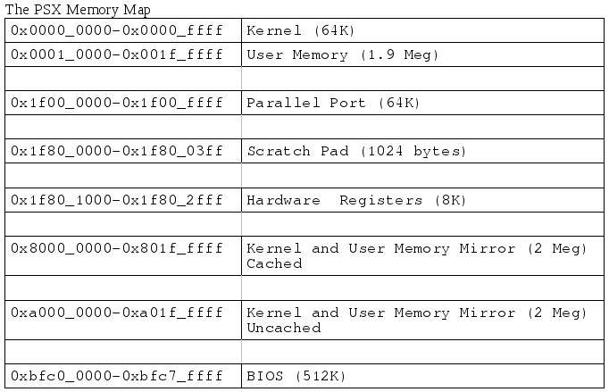
All blank areas represent the absence of memory. The mirrors are used mostly for caching and exception handling purposes The Kernel is also mirrored in all three user memory spaces.
Virtual memory
The PSX uses a memory architecture known as “Virtual Memory” to help with general system memory and cache management. In a nutshell what the PSX does is mirror the two meg of addressable space into 3 segments at three different virtual addresses. The names of these segments are Kuseg, Kseg0, and Kseg1.
Kuseg spans from 0x0000_0000 to 0x001f_ffff. This is what you might call “real” memory. This facilitates the kernel having direct access to user memory regions.
Kseg0 begins at virtual address 0x8000_0000 and goes to 0x801f_ffff. This segment is always translated to a linear 2MB region of the physical address space starting at physical address 0. All references through this segment are cacheable. When the most significant three bits of the virtual address are “100”, the virtual address resides in kseg0. The physical address is constructed by replacing these three bits of the virtual address with the value “000”.
Kseg1 is also a linear 2MB region from 0xa000_0000 to 0xa01f_ffff pointing to the same address at address 0. When the most significant three bits of the virtual address are “101”, the virtual address resides in kseg1. The physical address is constructed by replacing these three bits of the virtual address with the value “000”. Unlike kseg0, references through kseg1 are not cacheable.
Looking a little deeper into how virtual memory works, the following shows the anatomy of an R3000A virtual address. The most significant 20 bits of the 32-bit virtual address are called the virtual page number, or VPN. Only the three highest bits (segment number) are involved in the virtual to physical address translation.
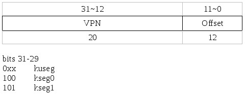
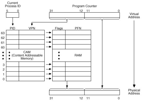
The three most significant bits of the virtual address identify which virtual address segment the processor is currently referencing; these segments have associated with them the mapping algorithm to be employed, and whether virtual addresses in that segment may reside in the cache. Pages are mapped by substituting a 20-bit physical frame number (PFN) for the 20-bit virtual page number field of the virtual address. This substitution is performed through the use of the on-chip Translation Lookaside Buffer (TLB). The TLB is a fully associative memory that holds 64 entries to provide a mapping of 64 4kB pages. When a virtual reference to kuseg each TLB entry is probed to see if it maps the corresponding VPN.
Virtual to physical memory translation
The following table is a quick look at how virtual memory gets translated via the Translation Lookaside Buffer. This whole subsystem of memory management is handled by Cop0.
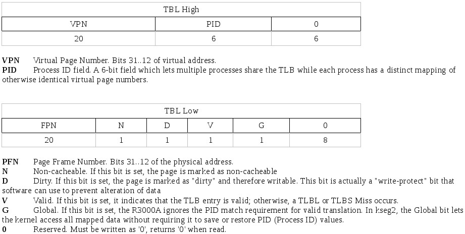
The System Control Coprocessor (Cop0)
This Unit is actually part of the R3000A. This particular cop0 has been modified from the original R3000A cop0 architecture with the addition of a few registers and functions. Cop0 contains 16 32-bit control registers that control the various aspects of memory management, system interrupt (exception) management, and breakpoints. Much of it is compatible with the normal R3000A cop0. The following is an overview of the Cop0 registers.
Note that some of these registers will be explained later in the part on exception handling. But for now we will return to how the Cop0 is used in memory management.
Returning to the TLB
As stated before the TLB is a fully associative memory that holds 64 entries to provide a mapping of 64 4kB pages. Each TLB entry is 64 bits wide. This is referenced by the Index, Random, TBL high, and TBL low. It is used to virtual to physical address mapping.
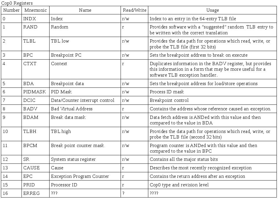
The Index Register
The Index register is a 32-bit, read-write register, which has a 6-bit field used to index to a specific entry in the 64-entry TLB file. The high-order bit of the register is a status bit which reflects the success or failure of a TLB Probe (tlbp) instruction.. The Index register also specifies the TLB entry that will be affected by the TLB Read (tlbr) and TLB Write Index (tlbwi) instructions. the following shows the format of the Index register.
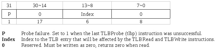
The Random Register
The Random register is a 32-bit read-only register. The format of the Random register is below. The six-bit Random field indexes a Random entry in the TLB. It is basically a counter which decrements on every clock cycle, but which is constrained to count in the range of 63 to 8. That is, software is guaranteed that the Random register will never index into the first 8 TLB entries. These entries can be "locked" by software into the TLB file, guaranteeing that no TLB miss exceptions will occur in operations which use those virtual address. This is useful for particularly critical areas of the operating system.
The Random register is typically used in the processing of a TLB miss exception. The Random register provides software with a "suggested" TLB entry to be written with the correct translation; although slightly less efficient than a Least Recently Used (LRU) algorithm, Random replacement offers substantially similar performance while allowing dramatically simpler hardware and software management. To perform a TLB replacement, the TLB Write Random (tlbwr) instruction is used to write the TLB entry indexed by this register. At reset, this counter is preset to the value '63'. Thus, it is possible for two processors to operate in "lock-step", even when using the Random TLB replacement algorithm. Also, software may directly read this register, although this feature probably has little utility outside of device testing and diagnostics.
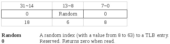
TBL High and TBL Low Registers
These two registers provide the data path for operations which read, write, or probe the TLB file. The format of these registers is the same as the format of a TLB entry.
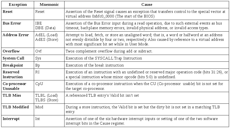
Exception Handling
There are times when in is necessary to suspend a program in order to process a hardware or software function. The exception processing capability of the R3000A is provided to assure an orderly transfer of control from an executing program to the kernel. Exceptions may be broadly divided into two categories: they can be caused by an instruction or instruction sequence, including an unusual condition arising during its execution; or can be caused by external events such as interrupts. When an R3000A detects an exception, the normal sequence of instruction flow is suspended; the processor is forced to kernel mode where it can respond to the abnormal or asynchronous event. The table below lists the exceptions recognized by the R3000A.
Returning to the Cop0
The Cop0 controls the exception handling with the use of the Cause register, the EPC register, the Status register, the BADV register, and the Context register. A brief description of each follows, after which the rest of the Cop0 registers for breakpoint management will be described for the sake of completeness.
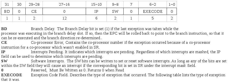
The Cause Register
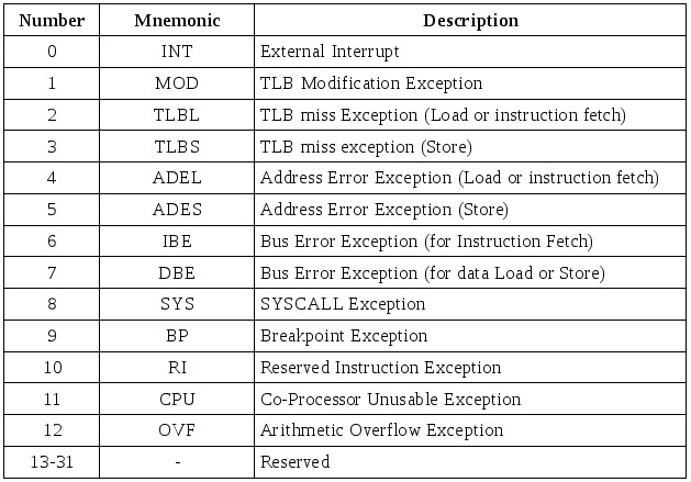
The contents of the Cause register describe the last exception. A 5-bit exception code indicates the cause of the current exception; the remaining fields contain detailed information specific to certain exceptions. All bits in this register, with the exception of the SW bits, are read-only.
The EPC (Exception Program Counter) Register
The 32-bit EPC register contains the virtual address of the instruction which took the exception, from which point processing resumes after the exception has been serviced. When the virtual address of the instruction resides in a branch delay slot, the EPC contains the virtual address of the instruction immediately preceding the exception (that is, the EPC points to the Branch or Jump instruction).
BADV Register
The BADV register saves the entire bad virtual address for any addressing exception.
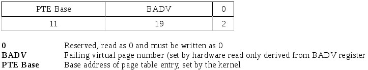
Context Register
The Context register duplicates some of the information in the BADV register, but provides this information in a form that may be more useful for a software TLB exception handler. The following illustrates the layout of the Context register. The Context register is used to allow software to quickly determine the main memory address of the page table entry corresponding to the bad virtual address, and allows the TLB to be updated by software very quickly (using a nine-instruction code sequence).
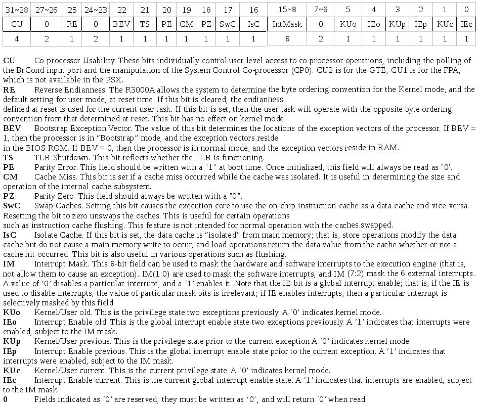
The Status Register
The Status register contains all the major status bits; any exception puts the system in Kernel mode. All bits in the status register, with the exception of the TS (TLB Shutdown) bit, are readable and writable; the TS bit is read-only. Figure 5.4 shows the functionality of the various bits in the status register. The status register contains a three level stack (current, previous, and old) of the kernel/user mode bit (KU) and the interrupt enable (IE) bit. The stack is pushed when each exception is taken, and popped by the Restore From Exception instruction. These bits may also be directly read or written. At reset, the SWc, KUc, and IEc bits are set to zero; BEV is set to one; and the value of the TS bit is set to 0 (TS = 0) The rest of the bit fields are undefined after reset.
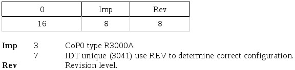
PRID Register
This register is useful to software in determining which revision of the processor is executing the code. The format of this register is illustrated below.
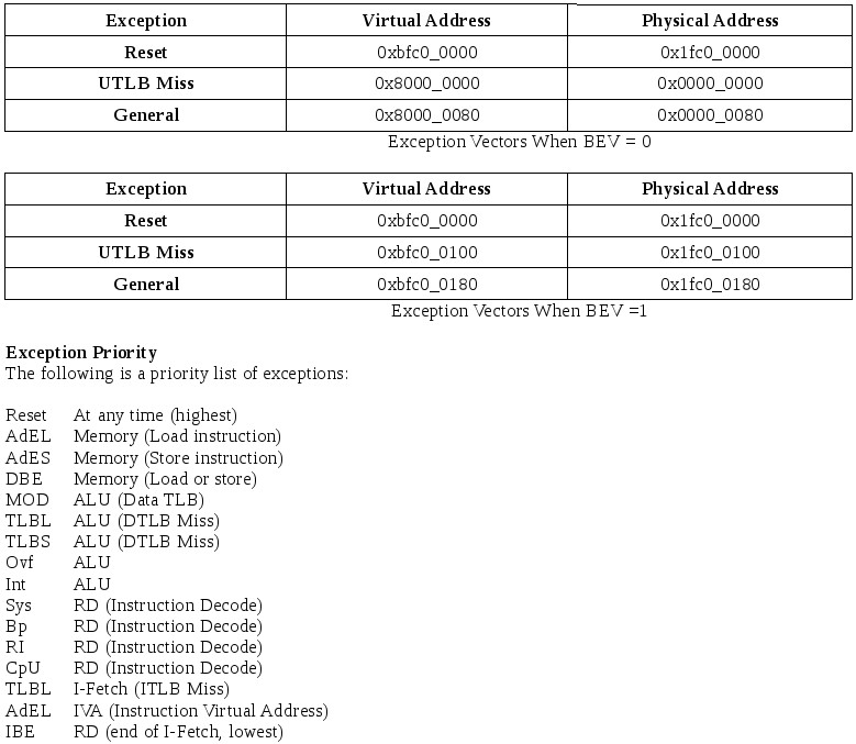
EXCEPTION VECTOR LOCATIONS
The R3000A separates exceptions into three vector spaces. The value of each vector depends on the BEV (Boot Exception Vector) bit of the status register, which allows two alternate sets of vectors (and thus two different pieces of code) to be used. Typically, this is used to allow diagnostic tests to occur before the functionality of the cache is validated; processor reset forces the value of the BEV bit to a 1.
Breakpoint Management
The following is a listing of the registers in Cop0 that are used for breakpoint management. These registers are very useful for low-level debugging.
BPC
Breakpoint on execute. Sets the breakpoint address to break on execute.
BDA
Breakpoint on data access. Sets the breakpoint address for load/store operations
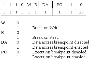
DCIC
Breakpoint control. To use the Execution breakpoint, set PC. To use the Data access breakpoint set DA and either R, W or both. Both breakpoints can be used simultaneously. When a breakpoint occurs the PSX jumps to 0x0000_0040.
BDAM
Data Access breakpoint mask. Data fetch address is ANDed with this value and then compared to the value in BDA
BPCM
Execute breakpoint mask. Program counter is ANDed with this value and then compared to the value in BPC.
DMA
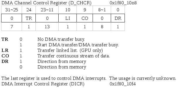
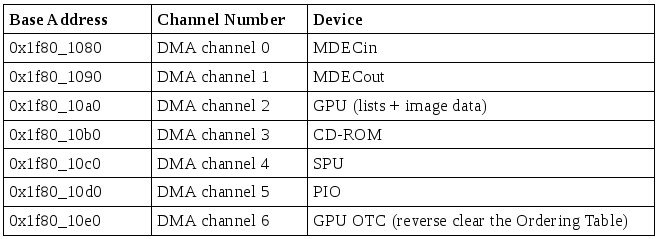
From time to time the PSX will need to take the CPU off the main bus in order to give a device access directly to Memory. The devices able to take control of the bus are the CD-ROM, MDEC, GPU, SPU, and the Parallel port. There are 7 DMA channels in all (The GPU and MDEC use two) The DMA registers reside between 0x1f80_1080 and 0x1f80_10f4. The DMA channel registers are located starting at 0x1f80_1080. The base address for each channel is as follows:
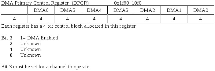
Each channel has three 32-bit control registers at a offset of the base address for that particular channel. These registers are the DMA Memory Address Register (D_MADR) at the base address, DMA Block Control Register (D_BCR)at base+4, and the DMA Channel Control Register (D_CHCR) at base+8.
In order to use DMA the appropriate channel must be enabled. This is done using the DMA Primary Control Register (DPCR) located at 0x1f80_10f0.
As stated above, each device has three 32-bit control registers within it’s own DMA address space. The following describes their functions. The n represents 8,9,a,b,c,d,e for DMA channels 0,1,2,3,4,5,6 respectively.
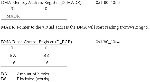
The channel will transfer BA blocks of BS words. Take care not to set the size larger than the buffer of the corresponding unit can hold. (GPU & SPU both have a $10 word buffer). A larger blocksize, means a faster transfer.