Building a register file isn't easy.
Chances to get hands on 74172 or AM29705 are low, same thing for synchronous
bi_port RAM.
Speaking of RAM, I did use a RAM in my M02 project for implementing the
registers, but nowadays buying fast SRAMs in DIP package would be going to
be tough. Also, correct timing for controlling 10nS RAM with 20ns TTL might
have its pitfalls. For more details, consult/dissect the schematics of my M02
project.
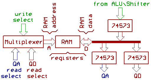
First a version with one RAM.
A multiplexer selects, what register to write, and what register to read into
the CPU internal address and data bus. The multiplexer is connected to the address
lines of the RAM. Also, we would need three 74573 buffers to handle the data while
reading/writing the RAM.
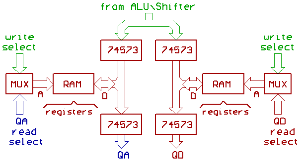
To make things faster, it's possible to run two RAMs in parallel.
(Writing into both RAMs happens simultaneously, so both RAMs will have the
same contents.)
Since there are fast 512 kB RAMs, one could implement large register windows
like with SPARC or AM29k. When going for a pipelined CPU, another idea
would be trying to run threads by hardware in parallel, for more details
consult/dissect the Innovasic Fido 1100 datasheet.
(Might give you some ideas for the FPGA implementation as well...)
Another idea might be integrating 512 kB memory into the CPU, with "data address
generators" like in SHARC DSPs to index the memory... and a third RAM that
contains the instructions.
All nice and fascinating ideas, but for our TREX CPU, we did decide to go with
things available in DIP package, what excludes the use of fast RAMs.
Now back to forming building blocks from premordeal slime...
Another idea would have been using the 74LS670, a 4 * 4 Bit RAM with separate
read/write ports. Building a fast 32 Bit register file with eight registers and
two separate data output ports would require 32 such ICs, but it's hard to tell
what the availability of the 74670 might look like in the future.
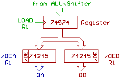
Well, there still is the 74574 8 Bit latch, which is supposed to stay in production
for a while. Imagine to have a "stack" of 74574s, with 18 of the 20 pins soldered
together: data inputs and outputs, GND and VCC. Control signals (load and output
enable) would be separate for each IC, of course.
You sure can imagine, that it might be possible to build sort of a "RAM" from such
devices.
...but we want to have two outputs for our "RAM".
One approach would be to attach two 74245 buffers to the outputs of each 74574,
so building a 32 Bit register file in the way we want would take 4 * 8 = 32 74574
and 4 * 8 * 2 = 64 74245, that's 192 ICs in total.
But since the 74574 has an output enable like the 74245 buffer, there would
be another approach:
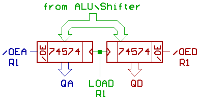
It would take 64 74574, and we did decide to take this approach.
It's funny, how the price for ICs goes down when ordering large quantities,
isn't it ?
Load factor issues (fan_in/fan_out) sure are important when building something
like that with 74LS parts, so we went for 74HCT instead.
Note, that this trick of connecting 74574s together also would work when using
counters. Having counters as registers sure would speed up post_increment or
pre_decrement addressing modes, but 74ALS869 counters are very expensive
and hard to get, and using GAL22V10 in large numbers will drain plenty of
current from the power supply.
Steve Chamberlin did a nice implementation for GAL22V10 based 8 Bit
up/down counters in his BMOW hobby CPU project.
[HOME] [UP]/ [BACK] [1] [2] [3] [4] [5] [6] [7] [8] [NEXT]
(c) Dieter Mueller 2007, 2008