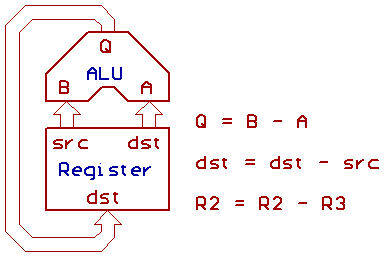
First some words on how to connect the 74181 to the registers:
'src' selects the source register, 'dst' the destination register.
Since "R2=R3-R2" would be highly impractical, and the 74181 doesn't support
B-A, the choice of how to place the register select is clear.
The design is spread over multible PCBs, and at some point during the design
phase, I lost the overview, and connected the external address and data bus
in the wrong way !
Sometimes it's hard to stay concentrated on your hobby projects over a long
time... when you happen to have a job and a life.
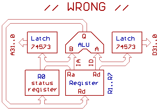
You see the problem.
If the Status Register output feeds the ALU B input, the CPU is unable of
writing the Status register directly to memory.
If the Status Register output would feed the ALU A input, it can't be the
destination of an ALU operation...
we wouldn't be able to do fast Bit manipulation on the output signals/ports
of the status register then !
Unfortunately, there wasn't enough PCB space left to have buffers
which allow feeding R0 into both ALU inputs.
And that's why you should transfer R0 into R6, and then write R6 to memory
instead, sorry for the inconvenience.
Other effects: if we would have a true bi_port register file, we would loose
cycles for post_increment memory access. So better change this when building
your own design.
Out of paranoia, PC is fed into both ALU inputs when incremented, same thing
for LA/R5 and the SKIP/CONT instruction. So this part of the design will work...
[HOME] [UP]/ [BACK] [1] [2] [3] [4] [5] [6] [7] [8] [NEXT]
(c) Dieter Mueller 2007, 2008