Now to take a closer look at what I found
when searching for publications related to
quantum dot cellular automata.
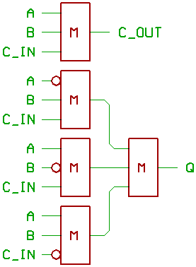
Tougaw and Lent, 1994:
Five majority gates...
and maybe three inverters.
Now to explain, how it works.
The carry chain isn't any different from
what we already know.
Now to dissect the rest which generates Q.
Remember: when one input of a three_input
majority gate is tied to 0, it turns into a
two_input AND, and when one of the three inputs
is tied to 1, it turns into a two_input OR.
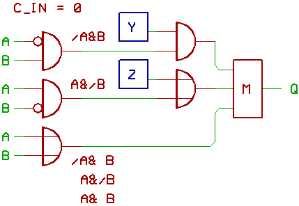
We now assume, that the carry input C_IN
is 0, and replace the first row of majority
gates with standard logic gates:
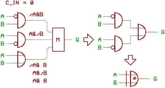
The first AND gate senses A=0 and B=1,
the second AND gate senses A=1 and B=0.
Since at least two inputs of the majority gate
have to be 1 to make it emitting 1 on Q,
we have this little OR gate attached,
which "enables" the majority gate if
A=0 and B=1, or A=1 and B=0.
The OR gate also produces 1 if A=1 and B=1,
but because the outputs of both ANDs are 0
in that case, we simply can ignore this fact.
When further simplifying the schematic,
the result is our well known XOR gate.
Now we assume that C_IN is 1...
and that the result will behave like
an XNOR gate, an inverted XOR.
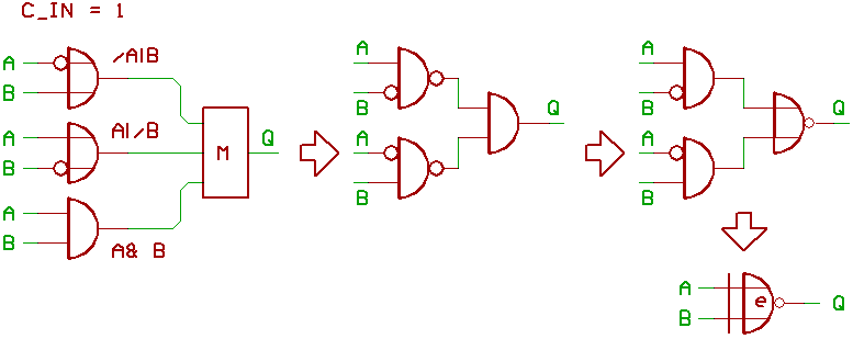
First to say, when you take an OR gate,
and replace it with an AND gate, you have
to invert all inputs and the output.
The schematic just looks more simple when
replacing the two OR gates with NANDs.
Now for the three gates in front of our
majority gate.
The first gate emits 0 when A=1 and B=0,
the second gate emits 0 when A=0 and B=1.
The third gate (AND) only emits 1,
when A=1 and B=1.
Because at least two inputs of our majority
gate have to be 1, the two NANDs force Q to 0
when A and B are not equal.
When simplifying this schematic further,
the end result is the XNOR gate we
expected from the start.
Now to describe, how to turn this into an ALU.
One Bitslice would look like this:
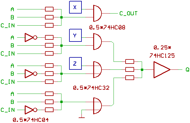
The blue boxes X, Y and Z are our control signals.
Arithmetic mode:
X=1, Y=1, Z=0
makes sure, that the circuitry works exactly
like the adder we have seen above.
Logic mode:
First, X=0 turns off the carry chain.
(Make sure, that the carry input of the
ALU is 0 in that case.)
Now to ignore the carry chain, and to focus
on the three majority gates, feeding the majority
gate at the Q output.
Since C_IN is 0, we remember the example we already
had on this page, and imagine that those three gates
behave like simple logic gates:
Q = A XOR B: X=0, Y=1, Z=0.
We already discussed on this page, why.
Q = A OR B: X=0, Z=1.
Z=1 forces one input of the majority gate to 1.
Said gate then passes through A OR B.
What happens in the circuitry around Y
doesn't matter, so Y could be 0 or 1.
Q = A AND /B: X=0, Y=0, Z=0.
Y=0 forces one input of the majority gate to 0.
So if the AND gate which senses A AND /B emits 1,
Q is 1 (because of the OR gate which senses
A OR B, two inputs of the majority gate are
1 in that case).
You sure noticed, that Q = A AND /B,
but because you would have some circuitry
outside the ALU for negating B when calculating
Q = A - B, it's simple to compensate this...
Now for another example.
[HOME] [UP]/ [BACK] [1] [2] [3] [4] [5] [6] [7] [8] [NEXT]
(c) Dieter Mueller 2009