First: later on this page, you may ask:
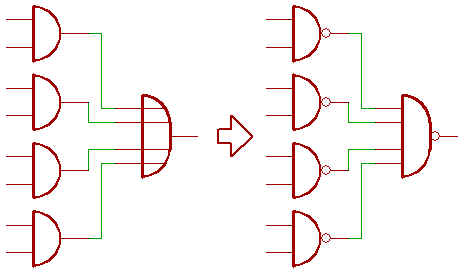
how to get OR gates with that much inputs ?
Answer: you could connect NAND gates together
like this:
But for better readability of those pictures,
I'll stick with AND OR combination gates
for the rest of this article.
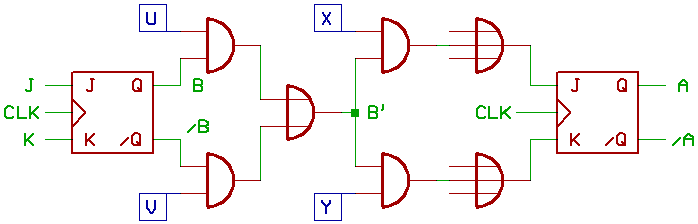
Now to build the part of the ALU, that performs
all the logic operations:
And yes, that's all.
B is a temporary storage register to hold the operand,
A is the accumulator.
One Bit bitslice shown in the picture.
The blue marked control signals U and V select,
if B' is 0, 1, B or /B.
The control signals X and Y select, what to do with the
accumulator Bit A.
To be more exact: if A should be set, reset or toggled
always at the rising edge of CLK, or only if B'=1.
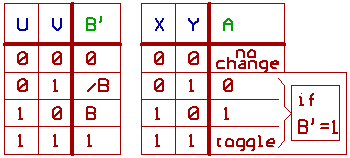
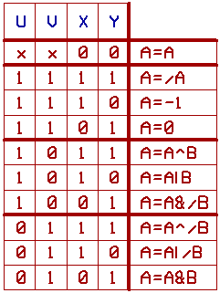
So the control lines give us a neat list of logic
operations for our ALU:
[HOME] [UP]/ [BACK] [1] [2] [3] [4] [5] [6] [7] [8] [NEXT]
(c) Dieter Mueller 2012