...and the question is:
what would it look like, when we are trying to build
a GAL22V10 based ALU from the things we learned
in this article so far.
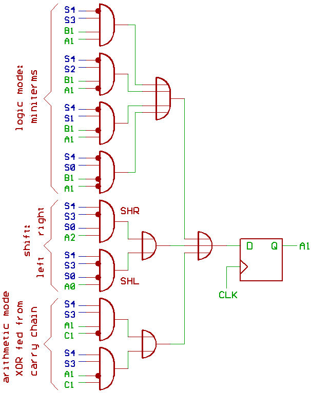
One Bit bitslice: (Bit 1 shown)
With only 8 product terms, the data path sure
is relatively small. Downside is, that arithmetic
operations usually take two steps (two clock cycles,
that is).
For logic operations, four AND gates are forming
a 4:1 multiplexer, as described in "ALU design, part 2".
S4=0 selects logic mode:

S3..0

 0000 Q=0
 1111 Q=-1 //all Bits set

 1010 Q=A
 1100 Q=B
 0101 Q=/A
 0011 Q=/B

 1110 Q= A| B
 1101 Q=/A| B
 1011 Q= A|/B
 0111 Q=/A|/B

 1000 Q= A& B
 0100 Q=/A& B
 0010 Q= A&/B
 0001 Q=/A&/B

 0110 Q=A^B
 1001 Q=/(A^B)
Two additional AND gates are needed for shifting the
accumulator Bits left or right.
To form an XOR gate for inverting the accumulator Bit
according to the carry input in arithmetic mode,
we need two more AND gates, and that's all.
[HOME] [UP]/ [BACK] [1] [2] [3] [4] [5] [6] [7] [8] [NEXT]
(c) Dieter Mueller 2012