First a short foreword:
I am aware, that the idea of building a transistorised CPU
may look a little bit strange/weird/eccentric.
If I want to do battle with FPGAs and RISC microcontrollers,
I could enjoy this every single day at work.
But imagine a time, far away in the future...
When CPLDs, FPGAs and microcontrollers would not have
any practical value for the hobbyist, and 74LSxx in DIP
package would be out of production.
(Or of too low/poor quality to be used in hobby projets.)
Would be nice, if we could build our own CPU
without proprietary hard/software.
Problem is:
When all you expect to have in the future would be
low_frequency transistors, model_railway transformers
and christmas_tree illuminations,
building your own CPU is going to be quite a challenge.
Comparing apples with pears may give incorrect results,
what also counts for comparing dynamic MOS circuitry
with a fully static bipolar design.
Nevertheless, transistor count for some CPUs
(found this in the internet):
4004 ( 4 Bit):  2300
8008 ( 8 Bit):  3300
8085 ( 8 Bit):  6200
8086 (16 Bit): 29000
MT15 (16 Bit), after some optimising, would contain
ca. 2800 transistors, LED drivers not counted.
So don't expect too much from this CPU, it may
never run any coloured windows.
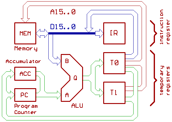
Now a block diagram of the MT15 data path.
MT15 data path is, basically, one big master/slave
flipflop, with multiple masters and slaves.
ACC, PC and program/data memory working as "master",
T0, T1 and flags working as "slave".
The grey box on the left represents program/data memory.
It isn't part of the CPU, address and date lines are
buffered with 74HCT245.
ACC is, basically, the "scratch_pad area",
PC is the program counter, pointing to the
next instruction to be fetched.
So far for the "masters". Now for the "slaves".
IR, instruction register, a 16 Bit transparent latch,
holding the OpCode during instruction execution.
T0,T1 are temporary registers, working as
ALU anti_race_latch for loading ACC,PC.
They also could connect to address and data bus.
While constructing the instruction set, it appeared
that data bus doesn't need to be written by T1.
Now to describe the clock circuitry.
[HOME] [UP]/ [BACK] [1] [2] [3] [4] [5] [6] [7] [8] [NEXT]
(c) Dieter Mueller 2005