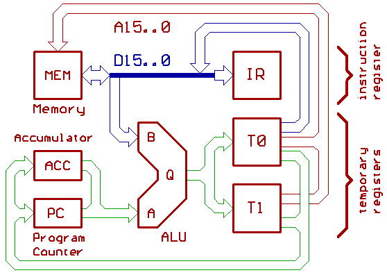
First to recall the MT15 data path:
Second, the MT15 instruction set:
 |15 14 13|12 11 10| 9| 8  7| 6| 5  4| 3  2  1  0|
 |--------|--------|--|-----|--|-----|-----------|
 |F2|F1|F0|A2|A1|A0|S |W1|W0|MF|M1|M0|C3|C2|C1|C0|
  -----------------------------------------------
  \ cond / \ addr / |  \ w / |  \cin/ \  alu    /
   ------   ------  |   ---  |   ---   ---------\
     |        |     |    |   |    |              \
     |        |     |    |   | 00 ALU_C_in=0      \
     |        |     |    |   | 01 ALU_C_in=C_Flag  |
     |        |     |    |   | 1x ALU_C_in=1       |
     |        |     |    |   |                     |   ALU_out =
000 true      |     |    | 0 keep___Flags     0000 AND reg& mem
001 if_I=1    |     |    | 1 modify_Flags     0001 ANN reg&!mem
010 if_N=0    |     |    |                    0010 ORA reg| mem
011 if_N=1    |     | 00 don't_write          0011 XOR reg^ mem
100 if_Z=0    |     | 01 write_ACC            0100 MVR reg
101 if_Z=1    |     | 10 write_PC             0101 MVM mem
110 if_C=0    |     | 11 write_memory         0110 DEC mem-1
111 if_C=1    |     |                         0111 SET $FFFF
              |     0 ALU_source=ACC          1000 CLR $0000
          000 #d16  1 ALU_source=PC           1001 ADD reg+mem
          001 #d16                            1010 SUB reg-mem
          010  d16+PC                         1010 SBU mem-reg
          011 [d16+PC]                        1100 SRR reg >>1
          100  d16+ACC                        1101 SRM mem >>1
          101 [d16+ACC]                       1110 SLR reg <<1
          110  d16                            1111 SLM mem <<1
          111 [d16]
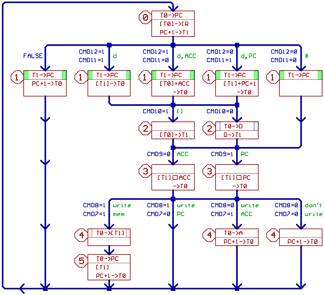
Now to define, what is supposed to happen when, how, and why.
Two things to clarify:
First, the red number in the yellow little boxes determines,
what step the state machine actually is in.
Second, not to forget, MT15 latches are transparent.
At the end of a step (that is one machine cycle), the ALU result
may be written into T0, or into T1.
Problem is, when loading ACC/PC with T0, result should be written in T1.
This also works in a reversed order: read T1, write T0.
Unfortunately, Read/write T0, or read/write T1 has to be avoided at any cost
...spoken literally.
Instruction execution happens in the following kind of order:
 Step 0  : fetch OpCode, RESET_FLAG and INT_FLAG.
 Step 1,2: prepare to fetch parameter, address calculation.
 Step 3  : data calculation, update status register (Flags).
 Step 4,5: write back result of data calculation.
Now to go more into detail.
Step 0: Opcode fetch.
Load Instruction Register (IR) from DataBus.
Load external RESET and INT signals into RESET_FLAG, INT_FLAG.
Prepare to increment Program Counter (PC), so it would point
to the parameter of the instruction.
Step 1: Skip/Execute, start address calculation.
If RESET is active, prepare to set PC to $0000 and goto Step 0.
(So PC is $0000, when reset goes inactive in step 0.)
Else, use the Flag_multiplexer (controlled by OpCode Bit 13..15),
to conditionally disregard or execute the instruction.
If FALSE (means, multiplexer output is 0), prepare to fetch
the next Instruction and goto Step 0.
Else, go on with instruction execution, and prepare to fetch
the parameter.
IF addressing mode is #, what means immediate, skip all further
address calculation and goto Step 3, that would be data calculation.
For all the other remaining addressing modes:
Effective Address (EA) would be:
Step 2: direct/indirect.
Effective Address has to be stored into T1 at the end of this cycle.
If indirect, load T1 with contents of the word in memory indicated
by the result from step 1.
Else, transfer the result from step 1 into T1 (the blue, inefficient
looking box).
Step 3: Data calculation.
T1 points to a word in memory, that is send into the ALU, together
with a register (ACC or PC).
Status_Register (Flags N,Z,C) may be modified by the result.
If the result of this data calculation shall be written into PC
(the "JUMP" instruction), we just go back to step 0,
without incrementing PC.
Step 4: write back
What means, decide what else to do with the result.
Result could be thrown away (perhaps for comparing two numbers,
what should only modify the flags), or written back into ACC.
In those two cases, we could now prepare to fetch the next instruction,
and go back to step 0.
The result could also written back to memory, what requires two
steps (step 4,5).
Note, that the address to be written to is stable for the step before
and after the write cycle (that red box).
Found it important, to have the address clean while writing.
After that, we go back to step 0 for fetching the next instruction.
And that's all.
Woud be a good idea, if you are going print out this page,
before we start digging into the five PLAs at transistor level
at the next five pages of this article, wouldn't it ?
[HOME] [UP]/ [BACK] [1] [2] [3] [4] [5] [6] [7] [8] [NEXT]
(c) Dieter Mueller 2005