PLA1 controls the sequencer, and read/write signals
for the data_bus to off_CPU program/data_memory.
Note:
+ means, no transistor.
O means, transistor (BC847 or BC857) at this location.
      !S0-O+++O++O++O+++++
       S0-+OOO+OO+OO++++++
      !S1-OOOO+++OOO++++++
       S1-++++OOO+++O+++++
      !S2-OOOOOOO+++O+++++
       S2-+++++++OOO++++++
     CMD7-++++++OOOO++++++
    !CMD8-+++++O++++++++++
     CMD8-++++++OOOO++++++
   !CMD11-+++O++++++++++++
    CMD11-+O++++++++++++++
   !CMD12-+++O++++++++++++
    CMD12-++O+++++++++++++
!RES_FLAG-+OOO++++++++++++
     TRUE-+OOO++++++++++++
    PHI11-+++++++++O++++++
   !CMD10-++++++++++O+++++
         -++++++++++++++++
          ||||||||||||||||
          O++OO++O++++++++-NS0
          +OOOO+++++++++++-NS1
          +++++OOO++++++++-NS2
          ++++++++++++++++-
          ++++++++++++++++-
          ++++++++++++++++-
          ++++++++++++++++-
          ++++++++++O+++++-!OUT
          ++++++++O+++++++-DIR
          +++++++++O++++++-WE
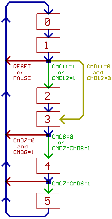
Now the state machine:
NS2..0 is the value to be loaded into S2..0 at the start
of the next machine cycle.
Note, that states not covered by this table will abort/terminate
instruction execution, and force a new instruction fetch.
Like in step 1, when RESET is active, or TRUE
(output of the flag multiplexer) is false/inactive.
 S2..0 !RES_FLAG TRUE CMD12 CMD11 CMD8 CMD7  NS2..0

 000   x         x    x     x     x    x     001   // 0->1
 001   1         1    x     1     x    x     010   // 1->2
 001   1         1    1     x     x    x     010   // 1->2
 001   1         1    0     0     x    x     011   // 1->3
 010   x         x    x     x     x    x     011   // 2->3 address calc./indirect
 011   x         x    x     x     0    x     100   // 3->4 write acc/NULL
 011   x         x    x     x     1    1     100   // 3->4 write mem
 100   x         x    x     x     1    1     101   // 4->5 write mem
Or, in a better readable form:
//fetch OpCode word

 0->1

//fetch parameter word, and start address calculation
//cycle trough state 2 and 3, if CMD12=1 or CMD11=1

 1->2 if TRUE, no RESET, CMD11=1
 1->2 if TRUE, no RESET, CMD12=1
 1->3 if TRUE, no RESET, CMD12=CMD11=0 //immediate: do data calculation

 2->3 //address calculation/indirect

//do data calculation, finished if "write result back to PC"

 3->4 if CMD8=0 //write acc/don't write


//write memory
 3->4 if CMD8=CMD7=1 //memory write enable active
 4->5 if CMD8=CMD7=1
Or, as a diagram:
The bus control:
 S2..0 CMD10 CMD8 CMD7 PHI11

 100   x     1    1    x    W   =1 //set data_bus drivers to "write"
 100   x     1    1    1    WE  =1 //write strobe
 010   0     x    x    x    !OUT=1 //disconnect external data_bus
Or, in another form:
   W=  S2 & !S1 & !S0 &  CMD8  & CMD7
  WE=  S2 & !S1 & !S0 &  CMD8  & CMD7 & PHI11
!OUT= !S2 &  S1 & !S0 & !CMD10
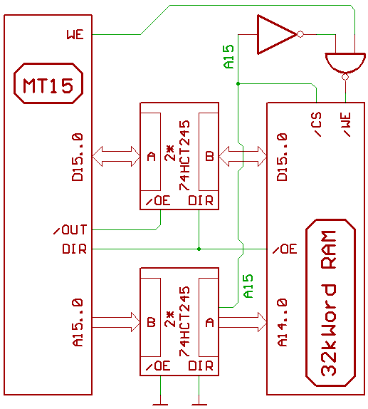
DIR=1 turns memory data_bus buffer to output (CPU -> memory)
WE=1 controls write enable of external memory
!OUT=1 disconnects internal CPU data bus from memory,
to transfer T0 into T1 trough CPU internal databus,
if there is no indirection during address calculation.
An example, how memory may be connected to MT15:
32 kWord RAM, located at address $0000...$7fff.
During MT15 test runs, I had
RAM at $0000...$7fff
I/O at $0800...$ffff
There wasn't any EPROM, because I used a PC parallel port (LPT)
to take over the bus and to read/write the RAM while MT15 RESET
was active.
[HOME] [UP]/ [BACK] [1] [2] [3] [4] [5] [6] [7] [8] [NEXT]
(c) Dieter Mueller 2005