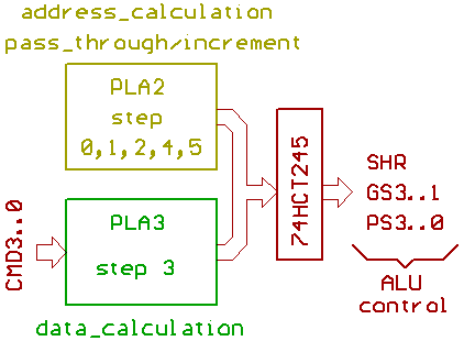
PLA3 works as a ROM, takes over ALU control
during data calculation (step 3).
OpCode Bit 0..3 is converted into 8 control signals:
PS0..3, GS1..3, SHR.
Note:
+ means, no transistor.
O means, transistor (BC847 or BC857) at this location.
    !S0-++++++++++++++++
     S0-OOOOOOOOOOOOOOOO
    !S1-++++++++++++++++
     S1-OOOOOOOOOOOOOOOO
    !S2-OOOOOOOOOOOOOOOO
     S2-++++++++++++++++
  !CMD0-O+O+O+O+O+O+O+O+
   CMD0-+O+O+O+O+O+O+O+O
  !CMD1-OO++OO++OO++OO++
   CMD1-++OO++OO++OO++OO
  !CMD2-OOOO++++OOOO++++
   CMD2-++++OOOO++++OOOO
  !CMD3-OOOOOOOO++++++++
   CMD3-++++++++OOOOOOOO
       -++++++++++++++++
       -++++++++++++++++
       -++++++++++++++++
       -++++++++++++++++
        ||||||||||||||||
        ++++++OO++OO++++-PS0
        +OOOO+OO+O++O+++-PS1
        ++OO+O+O+O+++O++-PS2
        O+O+OO+O++OOOO++-PS3
        ++++++++++++++++-GS0
        ++++++++++O+++O+-GS1
        ++++++O++++O+++O-GS2
        ++++++O++O++++OO-GS3
        ++++++++++++OO++-SHR
        ++++++++++++++++-
Note: for the next table,
mem is a short form for memory,
while reg means register.
 if S2..0 = 011 //step 3

 CMD3..0 SHR GS3..1 PS3..1  // ALU

 0000    0   000    1000    // Q = reg & mem
 0001    0   000    0010    // Q = reg &!mem
 0010    0   000    1110    // Q = reg | mem
 0011    0   000    0110    // Q = reg ^ mem //XOR
 0100    0   000    1010    // Q = reg
 0101    0   000    1100    // Q = mem
 0110    0   110    0011    // Q = mem-1     //decrement mem
 0111    0   000    1111    // Q = $FFFF     //-1
 1000    0   000    0000    // Q = $0000     // 0
 1001    0   100    0110    // Q = reg + mem
 1010    0   001    1001    // Q = mem - reg
 1011    0   010    1001    // Q = reg - mem
 1100    1   000    1010    // Q = reg >>1   //shift right reg
 1101    1   000    1100    // Q = mem >>1   //shift right mem
 1110    0   101    0000    // Q = reg <<1   //shift left  reg
 1111    0   110    0000    // Q = mem <<1   //shift left  mem
Note: use CMD5 for incrementing.
Outputs of PLA2 and PLA3 are wired together:
[HOME] [UP]/ [BACK] [1] [2] [3] [4] [5] [6] [7] [8] [NEXT]
(c) Dieter Mueller 2005